
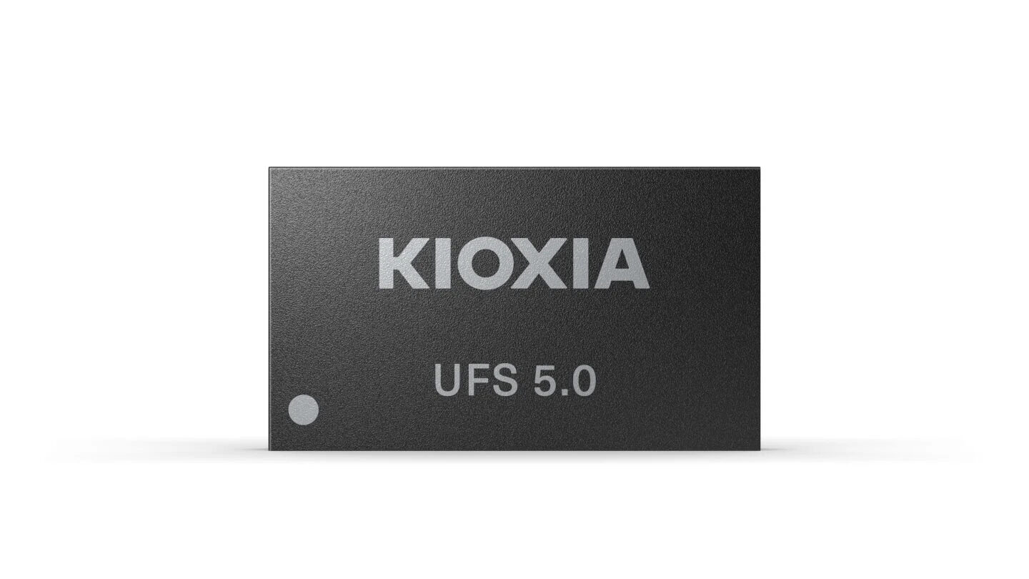
Kioxia begins sampling its latest UFS 5.0 flash memory, delivering faster speeds and enhanced power efficiency to support AI-driven, high-performance next-generation smartphones.
Kioxia Corporation has announced the commencement of evaluation sample shipments for its next-generation embedded flash memory solutions based on the emerging UFS 5.0 standard. The development marks a significant milestone in high-performance mobile storage technology, positioning the company at the forefront of next-generation semiconductor innovation designed to power advanced smartphones and AI-driven mobile devices.
Advancing Toward the UFS 5.0 Era
The Universal Flash Storage (UFS) standard continues to evolve in response to the increasing performance demands of modern mobile computing. As smartphones integrate more advanced features such as on-device artificial intelligence processing, high-resolution video recording, augmented reality applications, and real-time data analytics, storage subsystems must deliver substantially higher throughput, lower latency, and improved power efficiency.
UFS 5.0 is currently under development by JEDEC, the global semiconductor engineering standardization body responsible for defining memory and storage standards used across the electronics industry. The new UFS 5.0 specification is designed to significantly increase interface bandwidth while maintaining power efficiency suitable for mobile devices.
Kioxia’s newly introduced evaluation samples are built to align with these developing specifications, allowing system manufacturers to begin integration testing and performance validation in preparation for commercial deployment once the standard is finalized.
Designed for Next-Generation Mobile and AI Devices
The rapid rise of AI-enabled smartphones has transformed performance expectations for embedded storage. Modern flagship smartphones now execute complex AI workloads directly on the device—such as generative AI tasks, advanced image recognition, real-time language translation, and intelligent video processing—without relying solely on cloud infrastructure. These capabilities require extremely fast data transfer between memory, processors, and storage components.
UFS 5.0 addresses this need through a dramatic increase in interface speed. The new standard utilizes MIPI M-PHY version 6.0 for the physical layer and UniPro version 3.0 for the protocol layer. The integration of M-PHY version 6.0 introduces a new high-speed transmission mode known as HS-GEAR6. This mode theoretically enables a maximum interface speed of 46.6 gigabits per second (Gbps) per lane.
With two lanes operating simultaneously, UFS 5.0 can achieve an effective read/write performance of approximately 10.8 gigabytes per second (GB/s). This represents a substantial performance leap compared to previous UFS generations, enabling faster app launches, seamless multitasking, improved gaming performance, and significantly reduced data transfer times.
For consumers, this translates into smoother user experiences—instantaneous photo and video processing, rapid file downloads, quicker boot times, and enhanced AI responsiveness. For device manufacturers, it opens new opportunities to design feature-rich devices without storage bottlenecks limiting performance.
Newly Developed UFS 5.0 Controller Architecture
At the core of Kioxia’s evaluation samples is a newly developed controller engineered specifically for UFS 5.0 operation. The controller plays a critical role in managing data flow between the host processor and the flash memory, ensuring reliable high-speed communication while maintaining low power consumption and thermal efficiency.
This controller is optimized to handle the increased signaling speeds enabled by M-PHY version 6.0 while maintaining signal integrity and stability. High-speed data transmission at 46.6 Gbps per lane introduces engineering challenges related to noise, interference, and power efficiency. The newly designed controller addresses these challenges through advanced error correction, signal conditioning, and optimized firmware management.
By combining controller innovation with next-generation NAND memory, Kioxia aims to deliver both performance scalability and reliability suitable for flagship mobile platforms.
Integration of 8th Generation BiCS FLASH™
The evaluation samples incorporate Kioxia’s 8th generation BiCS FLASH™ 3D flash memory technology. BiCS FLASH™ is the company’s proprietary 3D NAND architecture, which stacks memory cells vertically to increase storage density while improving performance and power efficiency.
With each new generation, BiCS FLASH™ technology advances in layer count, cell architecture refinement, and process optimization. The 8th generation enhances write speeds, endurance characteristics, and power efficiency—critical attributes for mobile applications where battery life and thermal management are essential considerations.
The integration of 8th generation BiCS FLASH™ with the new UFS 5.0 controller enables the evaluation samples to achieve high bandwidth while maintaining reliability under demanding workloads such as continuous 8K video recording or AI model execution.
Capacity Options for Premium Devices
Kioxia’s UFS 5.0 evaluation samples are available in two capacity configurations:
- 512 gigabytes (GB)
- 1 terabyte (TB)
These capacity levels align with the growing storage requirements of high-end smartphones. With 4K and 8K video capture, high-resolution photography, and increasingly large AI models stored locally, device storage demands have expanded rapidly. A 1 TB mobile storage solution provides ample room for professional content creators, gamers, and AI-intensive applications.
Sample shipments of the 512 GB product begin on February 24, while the 1 TB version is scheduled for shipment in March. These samples are intended strictly for functional evaluation purposes. The final specifications of mass-produced products may differ once the UFS 5.0 standard is fully finalized and commercial production commences.
Compact Package for Space Efficiency
Beyond performance improvements, physical design efficiency remains a priority in mobile device engineering. The new UFS 5.0 package measures just 7.5 mm by 13 mm, offering a compact footprint that supports board space efficiency and flexible device layouts.
As smartphones become thinner and incorporate additional components such as larger camera modules, advanced cooling systems, and more complex antenna configurations, every millimeter of board space matters. A compact storage package enables manufacturers to optimize internal architecture, potentially allowing for larger batteries or additional performance components.
This compact design reflects Kioxia’s emphasis not only on performance, but also on practical system integration.
Collaboration with Host System Developers
Kioxia will ship UFS 5.0 samples to customers developing UFS 5.0-compatible host systems. This collaborative evaluation phase is essential in the semiconductor ecosystem, where memory vendors and system-on-chip manufacturers must validate interoperability and performance stability before mass production.
Performance verification and compatibility testing will ensure seamless integration between storage modules, application processors, and firmware stacks. Given the complexity of next-generation AI smartphones, early sampling allows ecosystem partners to fine-tune system architectures well ahead of commercial device launches.
This proactive sampling strategy supports faster time-to-market once UFS 5.0 becomes an industry-wide standard.
Understanding Performance Metrics and Capacity Calculations
Kioxia clarifies that the listed memory capacities reflect installed flash memory rather than user-available capacity. A portion of the total storage is reserved for management functions, firmware, wear leveling, and error correction. Therefore, actual usable storage may vary depending on product configuration.
Capacity calculations are based on binary measurement standards, where:
- 1 GB equals 1,073,741,824 bytes.
- 1 Gbps equals 1,000,000,000 bits per second.
- 1 GB/s equals 1,000,000,000 bytes per second.
These distinctions are important when comparing theoretical interface speeds to real-world performance outcomes, as actual data throughput depends on workload patterns, system design, and operating conditions.
Power Efficiency and Mobile Optimization
While performance increases are substantial, power efficiency remains a cornerstone of UFS development. Higher data rates often lead to increased power consumption, which can negatively affect battery life. UFS 5.0 is designed to balance throughput and energy efficiency through advanced signaling techniques and optimized protocol handling.
For AI-driven smartphones, energy-efficient storage is particularly critical. On-device AI workloads can run continuously, requiring sustained storage access. Efficient UFS 5.0 solutions help maintain performance without excessive thermal buildup or battery drain.
Strategic Vision for the Mobile Storage Market
Kioxia continues to emphasize its commitment to advancing flash memory technology in response to evolving market demands. By incorporating next-generation flash architectures into its UFS product lineup, the company aims to support higher capacities, faster performance, and enhanced reliability for premium mobile devices.
As mobile computing increasingly merges with AI acceleration, augmented reality, and high-performance gaming, storage subsystems must evolve from passive data repositories to high-speed performance enablers. UFS 5.0 represents a major step forward in that evolution.
The introduction of evaluation samples demonstrates readiness to support future smartphone platforms expected to launch in the coming product cycles. As JEDEC finalizes the UFS 5.0 specification, commercial production will likely follow, ushering in a new era of embedded flash performance.