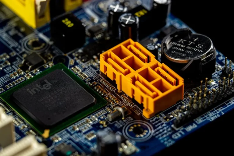


Dai Nippon Printing announced a significant technological milestone with the successful development of a nanoimprint lithography (NIL) template featuring an ultra-fine circuit line width of just 10 nanometers (nm). This achievement positions the company at the forefront of next-generation semiconductor manufacturing technologies. The newly developed NIL template supports patterning equivalent to logic semiconductors in the 1.4nm generation, a scale that aligns closely with the industry’s most advanced miniaturization requirements. With this breakthrough, DNP aims to address the growing need for high-precision, energy-efficient, and cost-effective semiconductor fabrication solutions amid accelerating global demand for cutting-edge chips.
The Global Push Toward Advanced Semiconductor Miniaturization
Across the semiconductor industry, continuous advancement in device performance has created escalating expectations for miniaturization, speed, and power efficiency. Over the past decade, these demands have intensified dramatically due to widespread adoption of technologies such as artificial intelligence (AI), 5G and 6G communications, autonomous driving, and edge computing. Each of these applications relies on logic semiconductors capable of supporting higher densities, increased processing throughput, and reduced energy consumption.
Extreme Ultra-Violet (EUV) lithography has emerged as the dominant method for producing such advanced, fine-pitch semiconductor devices. By using extremely short-wavelength light, EUV lithography enables manufacturers to print circuit patterns at scales previously unattainable with conventional deep ultraviolet (DUV) systems. However, despite EUV’s advantages, it also presents significant barriers. EUV scanners involve exceptionally high capital investment, often requiring billions of dollars for a single production line. Additionally, the energy consumption associated with generating and directing EUV light is substantial. The overall production process is complex, expensive, and often accessible only to a limited number of highly capitalized semiconductor manufacturers.
This gap has created a strong demand for alternative or complementary fabrication techniques that can achieve similar scaling benefits without incurring prohibitive costs. Many institutional, regional, and emerging semiconductor players—especially those without the infrastructure to support EUV—are actively exploring new methods. Among these, nanoimprint lithography has gained renewed interest as a cost-efficient patterning approach capable of producing extremely small, high-fidelity structures.
DNP’s Two Decades of NIL Development
DNP began its research and development efforts in nanoimprint lithography templates in 2003, long before NIL became a serious industry contender for advanced patterning. Over more than 20 years of continuous innovation, the company has built a deep foundation of expertise in micro- and nano-scale manufacturing, mastering the associated challenges of ultra-fine feature formation, structural durability, and reproducibility.
Key achievements throughout DNP’s development history include advances in:
- High-precision machining and etching technologies
- Template material optimization for durability and reliability
- Defect control and inspection methodologies
- Ultra-fine pattern uniformity over large areas
- Process integration with next-generation semiconductor workflows
This long-standing commitment has positioned DNP as one of the global leaders in NIL template production. The newly unveiled 10nm line pattern template represents the culmination of years of refinements and the latest addition to DNP’s portfolio of advanced semiconductor solutions.
Development of a 10nm Line Pattern NIL Template
The development of a NIL template capable of achieving a circuit line width at the 10nm scale represents a transformative step for the semiconductor industry. Producing patterns at this level of precision requires exceptional control over the fabrication environment, materials engineering, and pattern transfer techniques. Achieving 10nm line resolution places DNP’s NIL template within the performance category of cutting-edge logic technologies, such as those found in or beyond the 1.4nm semiconductor node.
The 10nm template enables the accurate replication of extremely fine patterns onto wafer substrates. Its performance pushes NIL technology into a realm that, until recently, was considered accessible primarily through EUV lithography. While NIL does not replace EUV entirely, the ability to substitute a portion of the EUV process offers significant advantages:
- Cost Efficiency: NIL equipment and production lines are far less expensive to build and operate than EUV lines.
- Energy Savings: NIL processing consumes considerably less energy, making it more environmentally sustainable.
- Process Flexibility: Manufacturers that lack EUV capabilities or wish to reduce EUV exposure steps can integrate NIL into existing flows.
- Scalability for Multiple Markets: NIL can be utilized not only for top-end logic chips but also for memory, photonic devices, and other applications that require nanoscale precision.
By enabling semiconductor manufacturers to adopt NIL for specific layers or steps in the patterning process, DNP offers a practical pathway to achieving next-generation performance without full reliance on EUV infrastructures.
Technical and Industrial Implications
The ability to pattern at the 10nm scale using NIL templates carries several major implications for semiconductor manufacturing and the broader technology ecosystem:
- Enhanced Device Density and Performance
Smaller line widths allow for more transistors to be packed into the same area, directly improving processing capability, energy efficiency, and overall device function. - Diversification of Manufacturing Methods
Manufacturers can reduce dependence on EUV and explore hybrid workflows that combine NIL and other lithography methods, enhancing resilience and flexibility in production planning. - Lower Barriers to Entry
Emerging semiconductor producers, universities, research labs, and specialized chip manufacturers can adopt NIL without requiring billions of dollars in infrastructure upgrades. - Global Supply Chain Stability
By offering a scalable alternative to EUV, NIL helps diversify global manufacturing routes and reduces bottlenecks tied to EUV tool availability. - Sustainability Benefits
Reducing reliance on energy-intensive processes contributes to carbon reduction goals and more sustainable semiconductor fabs.
DNP’s Future Vision for NIL Technology
DNP’s development of the 10nm NIL template marks a significant step toward enabling next-generation semiconductor production across a broader range of industry players. The company plans to continue pushing the boundaries of nanoimprint technology, with ongoing research focusing on further miniaturization, improved template durability, defect reduction, and greater pattern complexity.
Beyond logic semiconductors, DNP anticipates further opportunities in applications such as compound semiconductors, advanced optical components, and quantum devices—each of which requires extremely fine and precise pattern formation.
As demand for high-performance chips continues to surge globally, DNP aims to position NIL not only as an alternative to EUV, but as a mainstream, high-resolution patterning method capable of supporting the rapidly evolving needs of the semiconductor industry.
Source Link:https://www.businesswire.com/